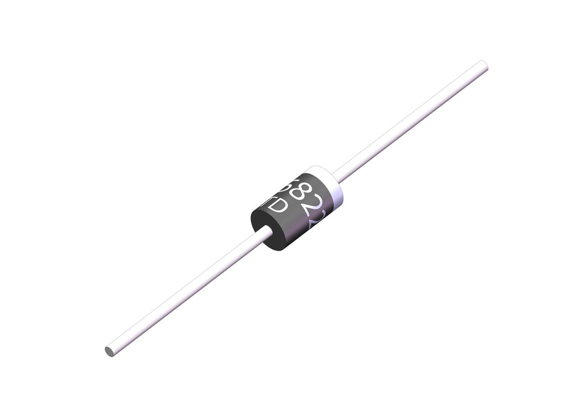
Send Message
Home ProductsSchottky Barrier Rectifier Diode

1N5820 1N5821 1N5822 Schottky Barrier Rectifier Diode IN5822 DO 27 Package

I'm Online Chat Now

1N5820 1N5821 1N5822 Schottky Barrier Rectifier Diode IN5822 DO 27 Package

1N5820 1N5821 1N5822 Schottky Barrier Rectifier Diode IN5822 DO 27 Package
1N5820 1N5821 1N5822 Schottky Barrier Rectifier Diode IN5822 DO 27 Package 1N5820 1N5821 1N5822 Schottky Barrier Rectifier Diode IN5822 DO 27 Package 1N5820 1N5821 1N5822 Schottky Barrier Rectifier Diode IN5822 DO 27 Package

Large Image :  1N5820 1N5821 1N5822 Schottky Barrier Rectifier Diode IN5822 DO 27 Package

Product Details:
Place of Origin: China
Brand Name: trusTec
Certification: ROHS
Model Number: 1N5820 THUR 1N5822
Payment & Shipping Terms:
Minimum Order Quantity: 1K PCS
Price: Negotiable (EXW/FOB/CNF)
Packaging Details: 1K PCS per tape & box, 10K PCS per carton.
Delivery Time: 10 work days fresh products
Payment Terms: T/T
Supply Ability: 800KK PCS per month

1N5820 1N5821 1N5822 Schottky Barrier Rectifier Diode IN5822 DO 27 Package

Description
Max. Reverse Voltage: 40V Max. Forward Current: 3A
Max. Forward Voltage: 0.5V Package: DO-27
Package Type: Through Hole Type: Schottky Diode
High Light:

1N5820 Schottky Diode

,

1N5821 Schottky Diode

,

1n5822 3a schottky diode

1N5820 THRU 1N5822
SCHOTTKY BARRIER RECTIFIERS
Reverse Voltage - 20 to 40 Volts Forward Current - 3.0 Ampere


Product size


1N5820 1N5821 1N5822 Schottky Barrier Rectifier Diode IN5822 DO 27 Package 0


MAXIMUM RATINGS
 
Ratings at 25 C ambient temperature unless otherwise specified.
Single phase half-wave 60Hz,resistive or inductive load,for current capacitive load derate by 20%.
 
  SYMBOLS 1N5820 1N5821 1N5822 UNITS
Maximum repetitive peak reverse voltage
VRRM
20
30
40
VOLTS
Maximum RMS voltage
VRMS
14 21 28
VOLTS
Maximum DC blocking voltage
VDC
20
30
40
VOLTS
Maximum average forward rectified current 0.375”(9.5mm) lead length at TL=90
I(AV)
3.0
Amp
Peak forward surge current 8.3ms single half sine-wave superimposed on rated load (JEDEC Method)
IFSM
25.0 Amps
Maximum instantaneous forward voltage at 1.0A
VF
0.450
0.550
0.600
Volts
Maximum DC reverse current TA=25
at rated DC blocking voltage TA=100
IR
0.5
10.0
mA
Typical junction capacitance (NOTE 1)
CJ
110.0
pF
Typical thermal resistance (NOTE 2)
RθJA
50.0
℃/W
Operating junction and storage temperature range
TJ,TSTG
-65 to +125
 
Note:
1.Measured at 1MHz and applied reverse voltage of 4.0V D.C.
2.Thermal resistance from junction to ambient at 0.375”(9.5mm)lead length,P.C.B. mounted


FEATURES
 
Plastic package has Underwriters Laboratory Flammability Classification 94V-0
Metal silicon junction,majority carrier conduction
Guardring for overvoltage protection
Low power loss,high erriciency
High current capability,low forward voltage drop
High surge capability
For use in low voltage,high frequency inverters, free wheeling,and polarity protection applications
High temperature soldering guaranteed: 260 C/10 seconds,0.375”(9.5mm) lead length, 5 lbs. (2.3kg) tension
 
MECHANICAL DATA
 
Case: JEDEC DO-201AD molded plastic body
Terminals: Plated axial leads, solderable per MIL-STD-750, Method 2026
Polarity: Color band denotes cathode end
Mounting Position: Any
Weight:0.04 ounce, 1.10 grams
 
RATINGS AND CHARACTERISTICS
 
Ratings at 25 C ambient temperature unless otherwise specified.
Single phase half-wave 60Hz,resistive or inductive load,for current capacitive load derate by 20%.
 
  SYMBOLS 1N5820 1N5821 1N5822 UNITS
Maximum repetitive peak reverse voltage
VRRM
20
30
40
VOLTS
Maximum RMS voltage
VRMS
14 21 28
VOLTS
Maximum DC blocking voltage
VDC
20
30
40
VOLTS
Maximum average forward rectified current 0.375”(9.5mm) lead length at TL=90
I(AV)
3.0
Amp
Peak forward surge current 8.3ms single half sine-wave superimposed on rated load (JEDEC Method)
IFSM
80.0 Amps
Maximum instantaneous forward voltage at 1.0A
VF
0.475
0.500
0.525
Volts
Maximum DC reverse current TA=25
at rated DC blocking voltage TA=100
IR
0.5
40.0
mA
Typical junction capacitance (NOTE 1)
CJ
300.0
pF
Typical thermal resistance (NOTE 2)
RθJA
40.0
℃/W
Operating junction and storage temperature range
TJ,TSTG
-65 to +125
 
Note:
1.Measured at 1MHz and applied reverse voltage of 4.0V D.C.
2.Thermal resistance from junction to ambient at 0.375”(9.5mm)lead length,P.C.B. mounted
 
Characteristic Curves
 

1N5820 1N5821 1N5822 Schottky Barrier Rectifier Diode IN5822 DO 27 Package 1

1N5820 1N5821 1N5822 Schottky Barrier Rectifier Diode IN5822 DO 27 Package 2

1N5820 1N5821 1N5822 Schottky Barrier Rectifier Diode IN5822 DO 27 Package 3

1N5820 1N5821 1N5822 Schottky Barrier Rectifier Diode IN5822 DO 27 Package 4

1N5820 1N5821 1N5822 Schottky Barrier Rectifier Diode IN5822 DO 27 Package 5

1N5820 1N5821 1N5822 Schottky Barrier Rectifier Diode IN5822 DO 27 Package 6

Contact Details
Changzhou Trustec Company Limited

Contact Person: Ms. Selena Chai

Tel: +86-13961191626

Fax: 86-519-85109398

Send your inquiry directly to us (0 / 3000)